This step-up voltage regulator consists of an isolated DC-to-DC power module in front of a step-up (boost) regulator. This enables up to 100 mA continuous at 12 V out from a 5 V input with full galvanic isolation between the input and output.
Special Order
Shipping from $4.90
+60 more from our supplier in 7-10 days
Our Code: SKU-011395
Supplier Link: [Pololu MPN:5759]
This step-up voltage regulator consists of an isolated DC-to-DC power module in front of a step-up (boost) regulator. This enables up to 100 mA continuous at 12 V out from a 5 V input with full galvanic isolation between the input and output. The 5 V, 300 mA output of the isolation IC is also available.
| Input voltage | Output voltages | Max continuous output current | Size |
|---|---|---|---|
| 4.5 V to 5.5 V | 12 V | 100 mA* | 0.4″ × 1.0″ |
| 5 V | 300 mA* |
* Max current per channel when the other channel current is zero.
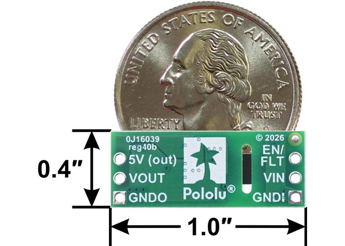
12V, 100mA Isolated Step-Up Voltage Regulator U5Z6F12, bottom view with dimensions and a US quarter for size reference.
This step-up voltage regulator consists of a Texas Instruments UCC33420RAQR isolated DC-to-DC power module followed by a 12 V boost regulator on the output side, enabling up to 100 mA continuous at 12V out from a 5 V input with full galvanic isolation between the input and output. The 5 V output of the UCC33420 that powers the boost regulator is also brought out, which can provide up to 300 mA continuous when there is no 12 V current draw (using the 5 V output will reduce available current from the 12 V output). Unlike non-isolated regulators, the output ground (GNDO) is effectively independent of the input side (GNDI), which can be useful for preventing ground loops and avoiding ground currents that can cause unpredictable system behaviour or even lead to damage to potentially expensive components.
Here are some of the regulator’s key features:
The board does not have built-in protection against reverse voltage, but reverse-voltage protection modules are available for adding that functionality.

Pinout of the 12V, 100mA Isolated Step-Up Voltage Regulator U5Z6F12.
| Side | Pin | Description |
|---|---|---|
| Input | VIN | 5 V input power supply. The regulator operates from 4.5 V to 5.5 V. Note that the input current will need to be around 600 mA to get 100 mA out at 12 V. |
| GNDI | Ground connection for VIN. GNDI is NOT connected to GNDO. | |
| EN/FLT | UCC33420 multi-function enable input and fault output. This connects directly to the EN/FLT pin on the input side of the UCC33420 and is pulled up to VIN through a 100 kΩ resistor. • Enable input: Driving this pin low disables the regulator and puts it into a low power state where it draws under 230 µA. The default state of this pin is high, which enables the regulator. • Fault output: The UCC33420 pulls this pin low for 200 µs if an output under-voltage or thermal protection fault occurs. |
|
| Output | VOUT | Regulated and isolated 12V output. |
| 5V (out) | This pin provides direct access to the UCC33420 isolated 5V (VCC) output, which is also used as the input to the output-side boost regulator. | |
| GNDO | Ground connection for VOUT and 5V (out). GNDO is NOT connected go GNDI. |
The connections are labelled on the back side of the PCB and are arranged with a 0.1″ spacing along the edges of the board for compatibility with solderless breadboards, connectors, and other prototyping arrangements that use a 0.1″ grid. You can solder wires or 0.1″ header pins directly to the board. Note: header pins are not included with this product, but straight and right-angle male headers are available separately.
We manufacture these boards in-house at our Las Vegas facility, so we can make these regulators with customised components to better meet the needs of your project, such as by customising the output voltage between 5.5 V and 28 V (though please note that the available current decreases significantly at higher output voltages). If you are interested in customisation, please contact us.
The efficiency of a voltage regulator, defined as (Power out)/(Power in), is an important measure of its performance, especially when battery life or heat are concerns. The graph below shows the efficiencies of the VOUT (12 V) output as a function of output current:

Typical efficiency of the U5Z6F12 12V output as a function of output current.
Please note that as this module consists of two chained regulators and includes isolated power transfer, the efficiency is around 50%, which is much lower than our non-isolated switching voltage regulators. The efficiency of the 5 V output is slightly higher since that does not go through the boost stage, but it is still below 60%.
The quiescent current is the current the regulator uses just to power itself, and the graph below shows this as a function of the input voltage, including voltages outside the valid operating range of the device:
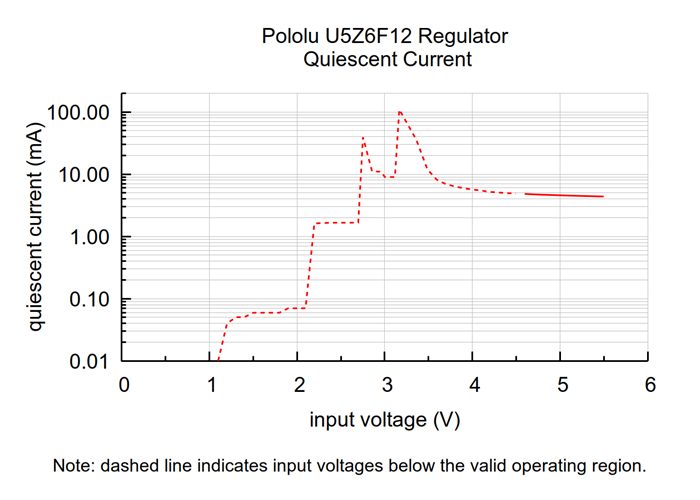
Typical quiescent current of the 12V, 100mA Isolated Step-Up Voltage Regulator U5Z6F12.
During normal operation, this product can get hot enough to burn you. Take care when handling this product or other components connected to it.
The UCC33420 provides basic isolation with a manufacturer-rated working voltage of 820 VRMS. The IC package has a clearance and creepage of >4.1 mm, and our PCB has a routed slot under the IC that increases the PCB creepage to 4.9 mm. A rough rule of thumb is that uncontaminated FR4 PCBs should have roughly 1 mm of creepage per 100 VRMS of isolation. Please note that our regulator module is not certified to any particular safety standard.
When connecting voltage to electronic circuits, the initial rush of current can cause voltage spikes that are much higher than the input voltage. In our tests with typical power leads (~30″ test clips), we observed spikes over 7.5 V with a 5 V input. Power supplies or leads with high inductance will make these spikes worse. An electrolytic capacitor (33 μF is a good starting point) can be added close to the regulator between VIN and GND to help suppress these spikes.
More information about LC spikes can be found in our application note, Understanding Destructive LC Voltage Spikes.
| Size: | 0.4″ × 1.0″ × 0.1″ |
|---|---|
| Weight: | 0.7 g |
| Minimum operating voltage: | 4.5 V |
|---|---|
| Maximum operating voltage: | 5.5 V |
| Maximum output current: | 100 mA |
| Output voltage: | 12 V1 |
| Reverse voltage protection?: | N |
| Isolated power transfer?: | Y |
| Working isolation voltage: | 820 VRMS2 |
| Maximum quiescent current: | 5 mA3 |
| PCB dev codes: | reg40b |
|---|---|
| Other PCB markings: | 0J16039 |
This DXF drawing shows the locations of all of the board’s holes.