Alchitry Pt V2

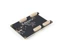
Experience platinum-tier performance with the Alchitry Pt V2, an FPGA board optimised for high-speed communication in a minimal footprint featuring the Xilinx Artix-7.

AUD$ 513.95

Special Order  

Shipping from $15.50

+22 more from our supplier in 7-10 days

Our Code: SKU-011045

Supplier Link: [SparkFun MPN:27873]


Description

The Flagship FPGA Development Board

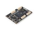
The Alchitry Pt V2 is a platinum-tier FPGA development board that has been engineered for high-speed performance and compact designs. The Pt V2 was designed with a low-profile backside, featuring no components taller than 1.5mm. This enables the use of high-speed 1.5mm stack-height DF40 connectors required by the high-speed GTP (gigabit transceiver port) capable of interfaces like PCIe 2.0.

Greater Performance with the Xilinx Artix-7 FPGA

At its core, the Alchitry Pt V2 is a powerhouse built for ambitious projects. It boasts:

  • A massive 101,440 logic cells, three times the resources of the Au V2.
  • 206 IO pins, nearly doubling the available amount on the Au V2.
  • Equipped with 240 dedicated DSP48E1 slices, perfect for demanding computational tasks.
  • 4,860 Kb of Block RAM Blocks, giving you the horsepower needed for complex applications like real-time signal processing and high-speed communication.

The Artix 7 FPGA requires a free licence for Vivado. Click here for instructions on installing it.

Stackable Expansion

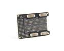
As part of the modular Alchitry ecosystem, the Pt stacks with expansion boards called "Elements" to add prototyping spaces, buttons, LEDs, and more. To make a proper physical connection with its high-speed connectors, the Pt requires a Br, Fn, or Sp Element when connecting to an Ft, Ft+, or Hd board. This prevents the connectors from contacting capacitors on the bottom of the Pt.


Specifications

  • XC7A100T-2FGG84I FPGA
  • Connectors on both sides of the board allow two independent stacks (IO isn't shared)
  • 206 IO pins
    • All IO pairs are LVDS_25 capable inputs or TMDS_33 capable IO
    • 112 on the top
      • 32 triple voltage (3.3V, 2.5V, or 1.8V) pins (16 pairs) capable of LVDS_25 IO
      • 76 routed as 100 ohm differential pairs
      • Remaining IO routed as 50 ohm single ended
      • 8 are on the control header
    • 92 on the bottom
      • 24 routed as 100 ohm differential pairs
      • Remaining IO routed as 50 ohm single ended
      • 8 are on the control header
    • 2 on QWIIC connector
  • 20 GTP pins broken out on the bottom
    • 2 clock input pairs
    • 4 Tx pairs
    • 4 Rx pairs
    • 6.25 Gb/s bandwidth per pair
  • 100MHz oscillator
  • 8 general purpose LEDs
  • 1 button (typically used as reset)
  • 256MB DDR3L @ 800Mb/s (400MHz)
  • 32MBit Configuration FLASH
  • FT2232HQ USB -> JTAG and USB -> UART (12Mbaud max) or FIFO (~8MB/s)
  • 5-12V input voltage on-board power supply
    • 3.3V @ 4A (IO)
    • 2.5V @ 500mA (triple voltage pins, derived from 3.3V)
    • 1V @ 4A (VCCINT)
    • 1.8V @ 1.2A (VCCAUX, triple voltage pins)
    • 1.35V @1.2A (DDR3L)
    • 1.8V @ 200mA (analogue)
    • 1V @ 1.5A (MGTAVCC, derived from 3.3V)
    • 1.2V @1.5A (MGTAVTT, derived from 3.3V)

Resources

Related Products