This power module is based on the MPS MIE1W0505BGLVH and provides regulated, galvanically isolated DC-to-DC power. The output voltage is set to 5 V by default and can be changed to 3.3 V through a selection pin.
Special Order
Shipping from $4.90
+610 more from our supplier in 7-10 days
Our Code: SKU-010763
Supplier Link: [Pololu MPN:5384]
This power module is based on the MPS MIE1W0505BGLVH and provides regulated, galvanically isolated DC-to-DC power. The output voltage is set to 5 V by default and can be changed to 3.3 V through a selection pin. Power specs:
| Input voltage | Output voltage | Max output current | Size |
|---|---|---|---|
| 4.5 V to 5.5 V | 5 V (default) or 3.3 V (selectable) | 200 mA | 0.3″ × 0.6″ |
| 3 V to 3.6 V | 3.3 V | 75 mA |
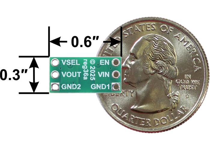
Isolated DC-DC Power Module, MIE1W0505BGLVH, 5V/3.3V, 200mA, basic dimensions with US quarter for size reference.
This DC-DC power module provides galvanically isolated (electrically isolated) and regulated 5 V or 3.3 V power at up to 200 mA. Unlike non-isolated regulators, the output ground (GND2) is effectively independent of the input side, which can be useful for preventing ground loops and avoiding ground currents that can cause unpredictable system behaviour or even lead to damage to potentially expensive components. This module is based on the MPS MIE1W0505BGLVH, which has a 2.5 kVRMS isolation rating; the PCB is designed with the same 3.5 mm minimum clearance and creepage between the isolated sides as the IC, but please note that the module itself is not certified to any standard. See the MIE1W0505BGLVH datasheet (624k pdf) for more information.
Here are some of the module’s key features:

Pinout of the Isolated DC-DC Power Module, MIE1W0505BGLVH, 5V/3.3V, 200mA.
Input power is supplied across VIN and GND1 and output power is delivered across VOUT and GND2. The two sides are galvanically isolated (GND1 is NOT connected to GND2). Note that the efficiency of this regulator is less than 50%, so the input power will need to be at least twice the output power.
| VIN range | VSEL | VOUT | Output current |
|---|---|---|---|
| 4.5 V to 5.5 V | NC (default) | 5 V | 180 mA continuous, 200 mA peak |
| GND2 | 3.3 V | ||
| 3 V to 3.6 V | GND2 | 3.3 V | 75 mA continuous |
The enable input, EN, is pulled up to VIN through a 100 kΩ resistor, which enables the regulator by default. This pin can be driven low to put the device into a low-power state where the shutdown current draw is typically dominated by the current through the pull-up resistor (10 µA per volt on VIN).
The output voltage selection pin, VSEL, is floating, which sets the output voltage to 5 V by default. To select 3.3 V for the output voltage, connect VSEL to GND2. This can be done using the board’s through holes or by adding an SMT jumper to the pads circled in the picture below. Note: The VCC voltage level is latched at power-up, so changing VSEL state while the board is powered will not have any effect until the board is power-cycled or enable is toggled.

An SMT jumper can be added here to connect VSEL to GND2, which sets VOUT to 3.3V.
We manufacture these boards in-house at our Las Vegas facility, so we can make these regulators with the jumper installed for 3.3 V output. Please contact us if you are interested in this customisation.
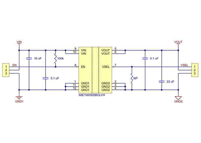
Schematic diagram of the Isolated DC-DC Power Module, MIE1W0505BGLVH, 5V/3.3V, 200mA.
| Size: | 0.3″ × 0.6″ × 0.1″ |
|---|---|
| Weight: | 0.5 g |
| Minimum operating voltage: | 3.0 V |
|---|---|
| Maximum operating voltage: | 5.5 V |
| Maximum output current: | 200 mA |
| Output voltage: | 5 V1 |
| Reverse voltage protection?: | N |
| Maximum quiescent current: | 11 mA2 |
| PCB dev codes: | reg36a |
|---|---|
| Other PCB markings: | 0J4042 |
This DXF drawing shows the locations of all of the board’s holes.
MPS product page for the MIE1W0505BGLVH, where you can find application notes and other resources.